Motherboard Chipsets and the Memory Map
I’m going to write a few posts about computer internals with the goal of explaining how modern kernels work. I hope to make them useful to enthusiasts and programmers who are interested in this stuff but don’t have experience with it. The focus is on Linux, Windows, and Intel processors. Internals are a hobby for me, I have written a fair bit of kernel-mode code but haven’t done so in a while. This first post describes the layout of modern Intel-based motherboards, how the CPU accesses memory and the system memory map.
To start off let’s take a look at how an Intel computer is wired up nowadays. The diagram below shows the main components in a motherboard and dubious color taste:
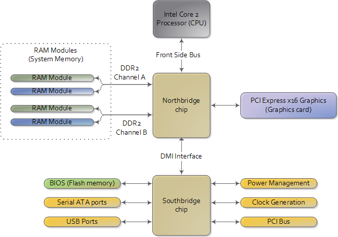
Diagram for modern motherboard. The northbridge and southbridge make up the chipset.
As you look at this, the crucial thing to keep in mind is that the CPU doesn’t really know anything about what it’s connected to. It talks to the outside world through its pins but it doesn’t care what that outside world is. It might be a motherboard in a computer but it could be a toaster, network router, brain implant, or CPU test bench. There are three main ways by which the CPU and the outside communicate: memory address space, I/O address space, and interrupts. We only worry about motherboards and memory for now.
In a motherboard the CPU’s gateway to the world is the front-side bus connecting it to the northbridge. Whenever the CPU needs to read or write memory it does so via this bus. It uses some pins to transmit the physical memory address it wants to write or read, while other pins send the value to be written or receive the value being read. An Intel Core 2 QX6600 has 33 pins to transmit the physical memory address (so there are 233 choices of memory locations) and 64 pins to send or receive data (so data is transmitted in a 64-bit data path, or 8-byte chunks). This allows the CPU to physically address 64 gigabytes of memory (233 locations * 8 bytes) although most chipsets only handle up to 8 gigs of RAM.
Now comes the rub. We’re used to thinking of memory only in terms of RAM, the stuff programs read from and write to all the time. And indeed most of the memory requests from the processor are routed to RAM modules by the northbridge. But not all of them. Physical memory addresses are also used for communication with assorted devices on the motherboard (this communication is called memory-mapped I/O). These devices include video cards, most PCI cards (say, a scanner or SCSI card), and also the flash memory that stores the BIOS.
When the northbridge receives a physical memory request it decides where to route it: should it go to RAM? Video card maybe? This routing is decided via the memory address map. For each region of physical memory addresses, the memory map knows the device that owns that region. The bulk of the addresses are mapped to RAM, but when they aren’t the memory map tells the chipset which device should service requests for those addresses. This mapping of memory addresses away from RAM modules causes the classic hole in PC memory between 640KB and 1MB. A bigger hole arises when memory addresses are reserved for video cards and PCI devices. This is why 32-bit OSes have problems using 4 gigs of RAM. In Linux the file /proc/iomem neatly lists these address range mappings. The diagram below shows a typical memory map for the first 4 gigs of physical memory addresses in an Intel PC:
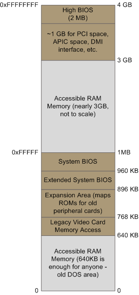
Memory layout for the first 4 gigabytes in an Intel system.
Actual addresses and ranges depend on the specific motherboard and devices present in the computer, but most Core 2 systems are pretty close to the above. All of the brown regions are mapped away from RAM. Remember that these are physical addresses that are used on the motherboard buses. Inside the CPU (for example, in the programs we run and write), the memory addresses are logical and they must be translated by the CPU into a physical address before memory is accessed on the bus.
The rules for translation of logical addresses into physical addresses are complex and they depend on the mode in which the CPU is running (real mode, 32-bit protected mode, and 64-bit protected mode). Regardless of the translation mechanism, the CPU mode determines how much physical memory can be accessed. For example, if the CPU is running in 32-bit mode, then it is only capable of physically addressing 4 GB (well, there is an exception called physical address extension, but ignore it for now). Since the top 1 GB or so of physical addresses are mapped to motherboard devices the CPU can effectively use only ~3 GB of RAM (sometimes less - I have a Vista machine where only 2.4 GB are usable). If the CPU is in real mode, then it can only address 1 megabyte of physical RAM (this is the only mode early Intel processors were capable of). On the other hand, a CPU running in 64-bit mode can physically access 64GB (few chipsets support that much RAM though). In 64-bit mode it is possible to use physical addresses above the total RAM in the system to access the RAM regions that correspond to physical addresses stolen by motherboard devices. This is called reclaiming memory and it’s done with help from the chipset.
That’s all the memory we need for the next post, which describes the boot process from power up until the boot loader is about to jump into the kernel. If you’d like to learn more about this stuff, I highly recommend the Intel manuals. I’m big into primary sources overall, but the Intel manuals in particular are well written and accurate. Here are some:
- Datasheet for Intel G35 Chipset documents a representative chipset for Core 2 processors. This is the main source for this post.
- Datasheet for Intel Core 2 Quad-Core Q6000 Sequence is a processor datasheet. It documents each pin in the processor (there aren’t that many actually, and after you group them there’s really not a lot to it). Fascinating stuff, though some bits are arcane.
- The Intel Software Developer’s Manuals are outstanding. Far from arcane, they explain beautifully all sorts of things about the architecture. Volumes 1 and 3A have the good stuff (don’t be put off by the name, the “volumes” are small and you can read selectively).
- Pádraig Brady suggested that I link to Ulrich Drepper’s excellent paper on memory. It’s great stuff. I was waiting to link to it in a post about memory, but the more the merrier.
Comments
28 Responses to “Motherboard Chipsets and the Memory Map”
Leave a Reply
[...] previous post described motherboards and the memory map in Intel computers to set the scene for the initial phases of boot. Booting is an involved, hacky, [...]
Very nice summary thanks.
I think it’s worth referencing Ulrich Drepper’s paper on memory,
which goes into more detail: http://people.redhat.com/drepper/cpumemory.pdf
Pádraig: absolutely
I’m a big fan of that paper too. I was waiting to reference it in an upcoming post about virtual memory / memory hierarchy, but it’s worth mentioning twice, so I’ll add it here too. Thanks for the suggestion.
Thanks for the summary. It was clear and very helpful. I was wondering where my 4GB of memory went.
[...] portion of the address space (that last 0.5GB for me) to communicate with these other devices (read this); therefore, it’s not mapped to RAM. Apparently, XP once supported PAE, an Intel hack that [...]
hi Gustavo, which software did you use to draw the diagrams?
Gustavo, conheci seu site hoje, gostei muito dessa parte teórica, já adicionei ao meu del.icio.us, vou visita-lo sempre…
agora deixa eu ir pq tenho mais coisas interessantes a ler aqui hehehe
@me: you’re welcome, glad it helped!
@kevin: Microsoft Visio 2007 - I wish it had been an open source tool. I use “themes” in Visio, which apply styles to all of the shapes, easing the process of creating something that looks ok.
@Fred: valeu, obrigado pelo comentario
Eh legal ver comentarios do pessoal do Brasil - eu mesmo estou querendo morar ai de novo por uns tempos. Se voce usar algum leitor de RSS, adicione o site.
[...] Duarte’s blog has some concise well written articles on, I particularly like the post on Motherboard Chipsets and the Memory Map and language [...]
Interessante esse post, tmb sou um hobista em relação a “systems internals”.
Não conhecia esse artigo (pelo tamanho tá mais pra livro) que foi citado “What Every Programmer Should Know About Memory”, mas parece ser muito completo… vou separar aqui pra ler!
Uma dica: As milhares de páginas dos manuais da Intel podem parecer intransponíveis a primeira vista para o iniciante, recomendo o livro “Protected Mode Software Architecture” da MindShare.
Abraço e parabéns.
@Augusto: obrigado, e valeu pela sugestao. Abraco.
Hi, i liked your article very much because it’s a subject i’ve been wanting to know more on for a while. I’ve read it over and over and ther is something I still don’t understand. I have no knowledge at all on this and it may be why. The thing is that I can’t figure out why with 32bits OS the cpu can only adress 4GB ? I understand why in 64bit it makes 64GB ( using the maths from the beginning ) but by using 32 instead of 64 in the formula I don’t get 4
does the 2^33 varies depeding on the OS ? Thx anyway great blog!
Opa, eu de novo…
“An Intel Core 2 QX6600 has 33 pins to transmit the physical memory address (so there are 233 choices of memory locations) and 64 pins to send or receive data (so data is transmitted in a 64-bit data path, or 8-byte chunks). This allows the CPU to physically address 64 gigabytes of memory (233 locations * 8 bytes) although most chipsets only handle up to 8 gigs of RAM.”
acho que essas informacoes nao estao corretas (posso estar errado)…
ateh onde sei, esse processador, assim como os outros de sua familia tem 32 linhas de enderecamento em “modo normal” o que possibilita 4GB de memoria. (2^32 * 1 byte)
esse processador tmb suporta PAE (physical address extension), com esse recurso ativado, passam a ser 36 linhas de enderecamento, possibilitando 64GB. (2^36 * 1 byte)
o bus de dados transfere chunks de 64 bits, mas a memoria eh enderecada por bytes..
Ol10:
“The thing is that I can’t figure out why with 32bits OS the cpu can only adress 4GB ?”
2^32 Bytes = 4294967296 Bytes = 4194304 KB = 4096 MB = 4 GB
So, a 32 bit system can theoretically address up to 4 GB because that’s the maximum of 32 bit binary numbers.
A 64 bit system can theoretically address up to 2^64 Bytes so 16 exabytes. But as you see, there are practical constraints.
(chrizel’s explanation is right, we typed at the same time)
@Ol10: Hi there. There is a difference between what the CPU is _physically_ capable of addressing and what it is _logically_ capable of addressing.
The _physical_ stuff is determined by hard-core limits: the actual metal pins that stick out of the processor. It is _those_ pins that limit the CPU to 64 gigabytes. That is completely independent of the operating system or even the mode (real-mode, 32-bit protected, 64-bit) the CPU is running in. It’s a physical limit. That is the limit for which that little multiplication is done. There are 33 metal pins to transmit an address and 8 metal pins to send and receive data. So 2^33 * 2^3 = 2^36 = 64 GB.
The “unit” of transfer in this case is 8 bytes, that’s the smallest chunk of data the CPU can address on the physical bus. In actuality, the CPU usually works in terms of cache lines, which hold 64 bytes in the Core 2s. Due to performance, the CPU reads a whole cache line at a time. So if a program reads one byte, the CPU actually reads 64 bytes and stores them in the cache.
The 4-gb limit is logical, not physical. It happens because the registers and instructions in the CPU are limited to 32 bits _when it’s running in 32-bit mode_, which _does_ depend on the OS. Programs need to be able to address individual bytes in memory, so the “unit” of addressing is 1 byte. So _that_ equation becomes 2^32 addresses * 1 byte chunks = 2^32 bytes, or 4 GB total addressing.
I hope this helps. Thanks for reading.
@Augusto: bem vindo de novo. De uma olhada nessa explicacao ai de cima, pois acho que responde sua pergunta tb. Os numeros que menciono no artigo sao as propriedades fisicas do processador, o numero de pinos disponiveis para enderecamento (33 pinos) e dados (8 pinos). De uma olhada no Datasheet for Intel Core 2 Quad-Core para esses dados.
Esses limites entao sao fisicos, independentes do modo da CPU. No bus, nao eh possivel enderecar memoria por bytes, pois a performance seria abismal. Na pratica, a CPU lida com pedacos de 64 bytes de uma vez, que corresponde ao tamanho da cache line.
Faz sentido?
Ok thank you for explaining.
gustavo,
http://www.cpu-world.com/info/Pinouts/Pentium_4.html
esse diagrama mostra a pinagem do pentium4 (nao achei a do core 2 quad), como pode ser constatado existem 36 linhas de enderecamento (A0-A35) e 64 linhas de dados (D0-D63).
@Augusto: hmm, repare no diagrama que vc postou, o primeiro pino de enderecamento eh A3#, ele nao comeca do zero
heheh. Tricky. Vai de A3# a A35#. Voce pode vir isso pro Core 2 tb em
http://download.intel.com/design/processor/datashts/31559205.pdf
Motherboard Chipsets and the Memory Map…
Information on x86 architecture…
gustavo,
tens razao… nao tinha me apercebido disso! curioso…
mas isso tem uma explicacao… nao existe necessidade das linhas A0-A2.
“In a similar vein, although the x86 processors can address 64GB of RAM, requiring 36 address lines, there are only 33 address bits (A3 through A35) coming out of the chip. The low-order three bits needn’t be specified because in the memory addresses that get out to the RAM, by the processor they are always zero — RAM is always read and written in eight-byte lumps.”
em modo normal (com PAE desativado), sao usadas as linhas A3:A31 enderecando 4GB de memoria fisica. Com PAE ativado sao usadas todas as linhas e ai sim dah pra enderecar 64GB.
vivendo e aprendendo! hehe
[...] Motherboard Chipsets and the Memory Map, How Computers Boot Up i The Kernel Boot Process Za one koje zanima kako računala rade iznutra, Gustavo Duarte je napisao seriju članaka čiji je cilj objasniti kako se računalo zapravo “podiže”. Počinje s matičnim pločama i memorijom, završava na detaljnom opisu Linuxovog kernela i malo manje detaljnom opisu kernela Windowsa. [...]
Hi,
your pictorial diagram of the modern Intel CPU chip-set is really worth thousand words. And off course hat-off to your explanation(with diagram) of infamous 640k-1MB legacy memory holes of Intel physical address space.
Keep on hacking good diagrams!!!
cheers!!!
- sushil
@sushil: thanks! I’m actually thinking most of my posts are going to be this sort of technical post + diagrams. I really like doing them, glad they were helpful.
[...] Motherboard chipsets and the memory map [...]
[...] Motherboard chipsets and the memory map [...]
[...] Motherboard Chipsets and the Memory Map : Gustavo Duarte (tags: hardware architecture memory kernel computer reference) [...]
Thank you for your article.
[...] the chipsets that power Intel motherboards, memory is accessed by the CPU via the front side bus, which connects [...]